Hey all, sorry it has been a while for the #nakeddiefriday due to health reasons, but here we come again
-
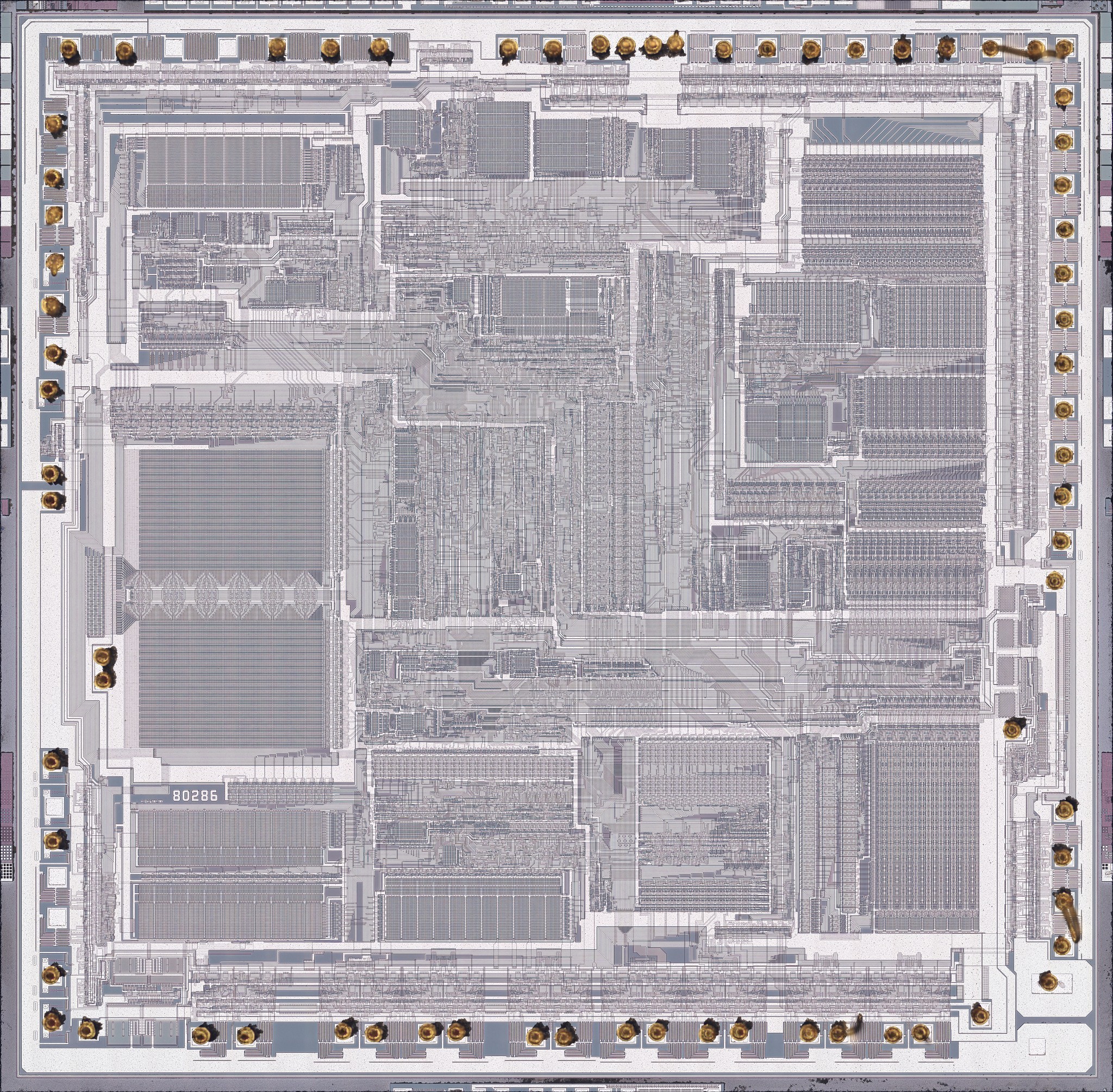
Quite unexpectedly, pin numbering on the die is going clockwise. Pin 1 is in top left corner of the image. I seem to recall some PLCC chips having dies mounted upside down...
Image taken from the AMD datasheet.
Note there are several "not connected" pins, which correspond to the unbonded pads. I wonder what signals are made available via those? If anyone has information, do comment please!
-
Note there are several "not connected" pins, which correspond to the unbonded pads. I wonder what signals are made available via those? If anyone has information, do comment please!
Now, there is a lot going on here on this die. Half the top and the whole right side of the pad ring is taken by the address bus pins. Visually tracing the wires shows the top right unit is connected to all of them. Probably not unrelated to the "address unit" on the block diagram.
-
Now, there is a lot going on here on this die. Half the top and the whole right side of the pad ring is taken by the address bus pins. Visually tracing the wires shows the top right unit is connected to all of them. Probably not unrelated to the "address unit" on the block diagram.
The whole bottom side is occupied by the 16 data bus pins. The wide bundle seems to be going up, so all the stuff around could be related to the datapath and instruction fetching. I got no idea where the ALU is.

-
The whole bottom side is occupied by the 16 data bus pins. The wide bundle seems to be going up, so all the stuff around could be related to the datapath and instruction fetching. I got no idea where the ALU is.
One thing easy to identify is the clock driver. Clock is probably the most important signal in any system, and one with the highest fanout. So it has to be driven with the biggest transistors. The deprocessed image clearly shows a lot of parallel structures.
-
One thing easy to identify is the clock driver. Clock is probably the most important signal in any system, and one with the highest fanout. So it has to be driven with the biggest transistors. The deprocessed image clearly shows a lot of parallel structures.
Another unit easy to identify--because it's right up in your face there--is the microcode ROM. It is the most densely packed unit of them all on this die. At the very top seems to be some registering and decoding action, splitting the inputs two ways: 8 bits goes to the left, the rest goes to the right. Bits on the left go into a small pre-decoder unit and produce 16 word lines. Bits on the right split again, and some 10 go into the middle of the array to produce two select lines per chunk, while another two drive the column muxes.
-
Another unit easy to identify--because it's right up in your face there--is the microcode ROM. It is the most densely packed unit of them all on this die. At the very top seems to be some registering and decoding action, splitting the inputs two ways: 8 bits goes to the left, the rest goes to the right. Bits on the left go into a small pre-decoder unit and produce 16 word lines. Bits on the right split again, and some 10 go into the middle of the array to produce two select lines per chunk, while another two drive the column muxes.
The microcode ROM outputs 17+18 lines, for the grand total of 35 bits. This seems obviously not enough to drive everything there is on the die, so some advanced magic must be going on. But this is a topic for deeper research. The implant ROM was not optically readable without further processing.
-
R AodeRelay shared this topic
-
The microcode ROM outputs 17+18 lines, for the grand total of 35 bits. This seems obviously not enough to drive everything there is on the die, so some advanced magic must be going on. But this is a topic for deeper research. The implant ROM was not optically readable without further processing.
Other structures are readable though. The whole die is full of PLAs. Let's have a closer look at them. Here's one, with pano links for convenience.
https://siliconprawn.org/map/intel/80286-10/infosecdj_mz_nikpa20x/#x=28132&y=5784&z=6
https://siliconprawn.org/map/intel/80286-10/infosecdj_poly_nikpa20x/#x=28133&y=5788&z=6 -
Other structures are readable though. The whole die is full of PLAs. Let's have a closer look at them. Here's one, with pano links for convenience.
https://siliconprawn.org/map/intel/80286-10/infosecdj_mz_nikpa20x/#x=28132&y=5784&z=6
https://siliconprawn.org/map/intel/80286-10/infosecdj_poly_nikpa20x/#x=28133&y=5788&z=6A programmable logic array (PLA) is a physical implementation of a bunch of logic equations, nothing more. It allows to flexibly "program" the outputs to become arbitrary logic functions of its inputs, in the form of "sum of products" typically. The "program" part happens at the design time though.
-
A programmable logic array (PLA) is a physical implementation of a bunch of logic equations, nothing more. It allows to flexibly "program" the outputs to become arbitrary logic functions of its inputs, in the form of "sum of products" typically. The "program" part happens at the design time though.
The products part is formed from the inputs by placing or skipping a transistor. Here are two product lines I drew over the previous image. Each vertical poly line represents an input, and each product is formed by connecting required inputs via a transistor to the product output! Nothing too complicated. Astute readers will notice each product is this formed by a NOR gate -- its pull-ups are on the right.
-
The products part is formed from the inputs by placing or skipping a transistor. Here are two product lines I drew over the previous image. Each vertical poly line represents an input, and each product is formed by connecting required inputs via a transistor to the product output! Nothing too complicated. Astute readers will notice each product is this formed by a NOR gate -- its pull-ups are on the right.
In this particular PLA, the sums are formed by discrete gates. Only about two products are used for each sum, so I guess this was a better solution area wise. Here is the schematics for that part. Q9..11 form another NOR gate which does the actual summing, while the rest appears to be signal conditioning and output driving. Counting inversions, it seems the output is the true sum of products of inverted inputs, as the designer only had NOR gates to work with... so NOR -> NOT-AND for the products, and then NOR-NOT-NOT-NOT -> OR for the sums.
-
In this particular PLA, the sums are formed by discrete gates. Only about two products are used for each sum, so I guess this was a better solution area wise. Here is the schematics for that part. Q9..11 form another NOR gate which does the actual summing, while the rest appears to be signal conditioning and output driving. Counting inversions, it seems the output is the true sum of products of inverted inputs, as the designer only had NOR gates to work with... so NOR -> NOT-AND for the products, and then NOR-NOT-NOT-NOT -> OR for the sums.
There are variations on the theme all over the die. In this particular instance, some of the inputs are routed through and out of the top for some other piece of circuitry to use. And one of the products is shamelessly routed out of the array on the metal layer.
-
There are variations on the theme all over the die. In this particular instance, some of the inputs are routed through and out of the top for some other piece of circuitry to use. And one of the products is shamelessly routed out of the array on the metal layer.
A more classical approach is to use arrays for both products and sums. Here is an example of such: products on the top, sums on the bottom.
-
A more classical approach is to use arrays for both products and sums. Here is an example of such: products on the top, sums on the bottom.
Here they could've just used a bunch of gates, really. Not everything needs to be a PLA.